In Part 1, we covered computer architecture and how a processor works at a high level.
Part 2 explored the design and implementation of individual chip components.
How do you transform a pile of sand into an advanced processor?
Let’s find out.
This involves introducing carefully selected impurities into the silicon substrate to alter its conductivity.
The goal is to change the way electrons behave so that we can control them.
Just like there are two types of transistors, there are also two corresponding types of doping.
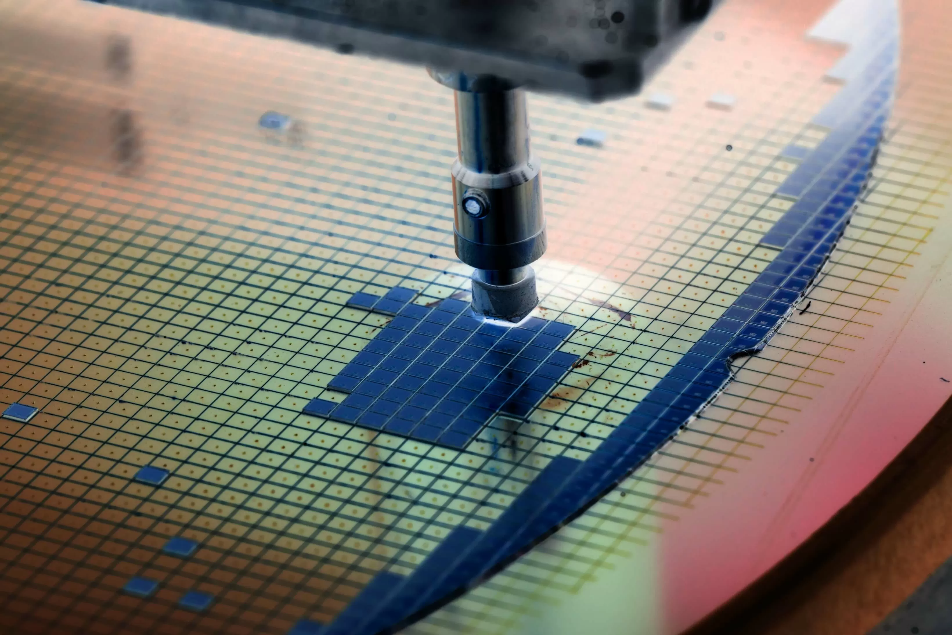
The fabrication process of a wafer before the chips are packaged.
This is where the name n-throw in and the “n” innMOScomes from.
This is where the “p” in p-key in andpMOScome from.
The current we are controlling flows through the Source and Drain.
The Gate is the switch used to turn the transistor on and off.
Finally, the Body of the gadget isn’t relevant to processor so we won’t discuss it here.
The physical structure of an inverter in silicon.
Each colored region has different conductivity properties.
A helpful analogy for how they work is a drawbridge over a river.
When we lower the drawbridge, we form a road over the river and the cars can move freely.
The same thing happens in a transistor.
Charging the gate forms a channel between the source and drain allowing current to flow.
Imagine a super-precise printer used to draw the patterns for each region onto the silicon.
As transistor sizes have shrunk, traditional deep ultraviolet (DUV) lithography has reached its limits.
A light-sensitive photoresist polymer is then applied over the silicon dioxide.
The wafer is then etched with hydrofluoric acid to dissolve the silicon dioxide where the photoresist was removed.
The remaining photoresist is stripped away, leaving behind just the oxide layer beneath.
The doping ions can now be applied to the wafer, selectively implanting themselves only in the exposed regions.
We’ll cover more about these connections and metal layers in a bit.
When a new chip is designed, they will generate masks for each step in the fabrication process.
These masks will contain the locations of each element of the billions of transistors on a chip.
Multiple chips are grouped together and fabricated at once on a single die.
Once a wafer is fabricated, the individual dies are sliced up and packaged.
Depending on the size of a chip, each wafer may fit hundreds or more chips.
As we increase the size of processors, the chance that a chip will be faulty increases.
One of the biggest marketing terms associated with chip fabrication is feature size or process node.
For example, TSMC is now working towards a “2nm” process.
Just a few years ago, 7nm and 10nm were considered pioneering technologies.
But what do these numbers actually mean?
Traditionally, the feature size referred to the minimum width between the drain and source of a transistor.
When examining these process nodes, it’s important to note that different companies define their sizes differently.
Additionally, not all transistors within the same fabrication process are the same size.
Designers may intentionally create some transistors larger than others, depending on specific performance requirements.
However, they can only drive a limited number of outputs due to their reduced current-handling capacity.
In some cases, output transistors can be orders of magnitude larger than the internal logic transistors.
A die shot of an AMD Zen processor.
Several billion transistors make up this design.
Designing and building the transistors is only half of the chip though.
We need to build wires to connect everything according to the schematic.
These connections are made using metal layers above the transistors.
Imagine a multi-level highway interchange with on-ramps, off-ramps, and different roads crossing each other.
That’s exactly what is going on inside a chip, albeit on a much smaller scale.
Different processes will have different numbers of metal interconnect layers above the transistors.
As transistors get smaller, more metal layers are needed to be able to route all the signals.
TSMC’s 5nm process has a reported 15 metal layers.
The microscope image below shows the lattice formed by seven metal layers.
Each layer is flat and as they go higher, the layers get bigger to help reduce resistance.
Each layer typically alternates in direction from the one below it to help reduce unwanted capacitances.
To help solve this issue, computer programs are used to automatically place and route the transistors.
For example, Intel or TSMC will provide designers with basic parts like logic gates or memory cells.
The designers can then combine these standard cells into whatever chip they want to build.
These layouts are turned into masks which are used in the fabrication process we covered above.
Next we’ll see what this design process might look like for an extremely basic chip.
First we see the layout for an inverter which is a standard cell.
The input A comes in on the left and the output Y goes out on the right.
The power and ground connections are made at the top and bottom on metal 2.
Combining several gates, here we have a basic 1-bit arithmetic unit.
This design can add, subtract, and perform logical operations on two 1-bit inputs.
The slashed blue wires that go vertically are metal 3 layers.
The slightly larger squares on the ends of the wires are vias that connect two layers.
Even at this small scale, the complexity is evident.
With that, our deep dive into processor fabrication comes to an end.
What are researchers working on now to make the next generation of computers even faster?
Masthead credit:Macro photo
