For those unfamiliar, Intel follows a “tick tock” model for its processor upgrade cycle.
Then, with an alternating “tock” cycle Intel introduces a new processor microarchitecture.
Ivy Bridge includes manufacturing and subsystem improvements.
This presents several benefits.
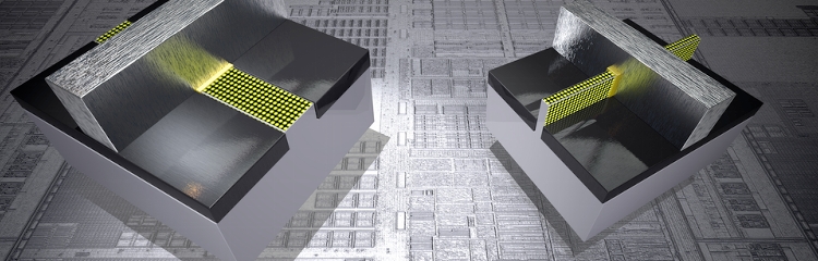
Transistors carry an electrical signal while gates control that flow by turning the current on and off.
The video below does a better job explaining this.
This design also maximizes transistor switching performance between on and off states and decreases power-wasting leakage.
The new 22nm Tri-Gate wafers shouldn’t be much more expensive to produce, either.
Besides the new transistor design there are no major changes in the Ivy Bridge architecture compared to Sandy Bridge.
To each side of this central portion is the system agent and the graphics core.
All these components are bound by a ring-bus that transports data between them.
Graphics
But there are also a few tweaks here and there.
This will finally bring the Intel integrated GPU to feature parity with AMD’s.
Ivy Bridge also greatly improves Intel Quick Sync Video, the chip giant’s transcoding technology.
Ivy Bridge also reportedly allows for more dynamic overclocking.
On the next two pages:Ivy Bridge’s power optimizations&CPU and chipset confirmed launch line-ups.
