Nvidia kept the Turing line going for two years before replacing it withAmperein September 2020.
But what about the chips powering them?
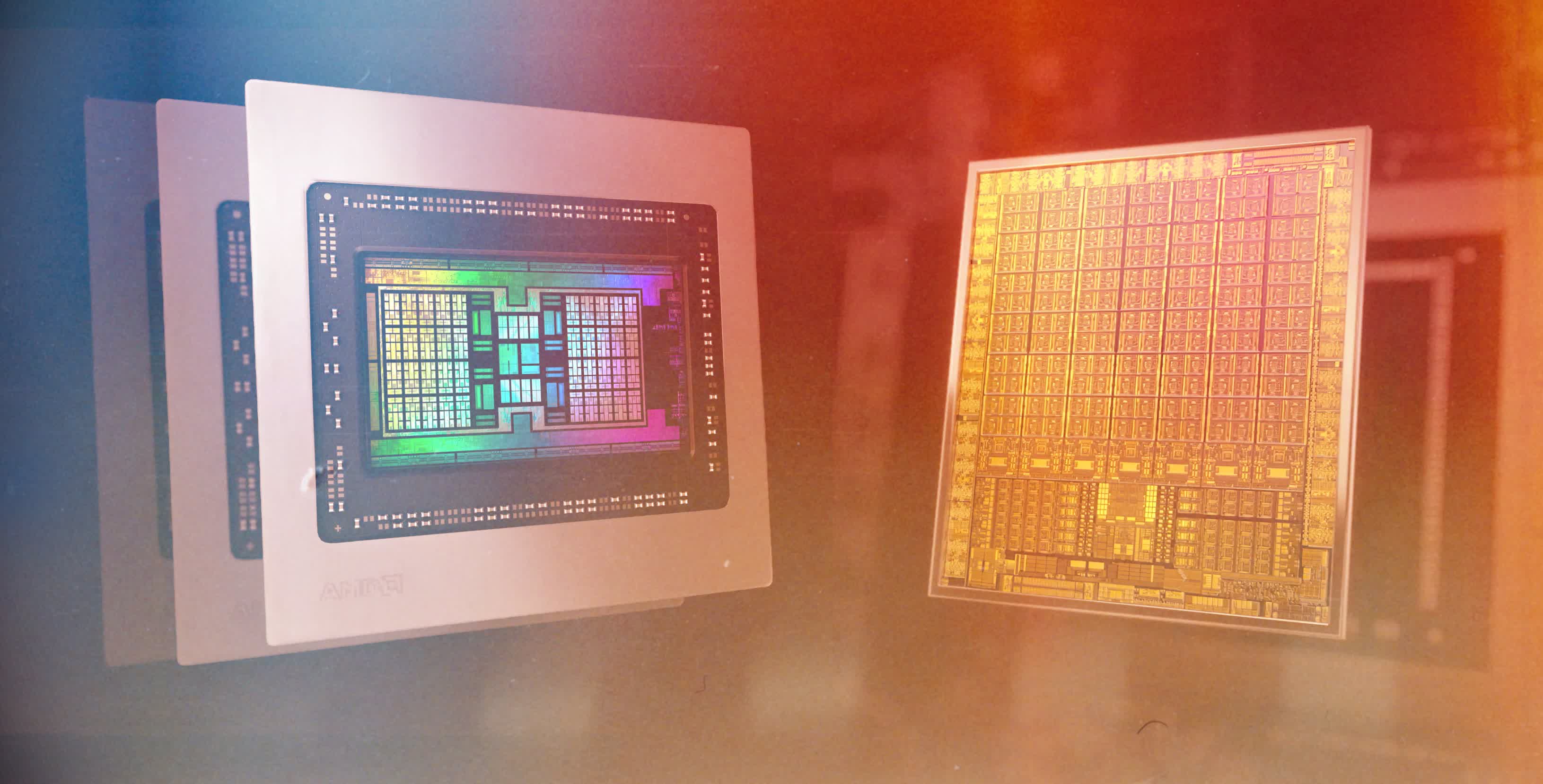
AMD’s latest offering is roughly 520 mm2in area, more than double the size of their previousNavichip.
It was 596 mm2in die area, but it was manufactured on TSMC’s 28HP process node.
The latest Ampere-based chip, the GA102, is 628 mm2.
Putting them all side-by-side highlights just how bulky Nvidia’s biggest GPUs are.
The Navi 21 looks fairly svelte, although there’s more to a processor than just die area.
So let’s dig into the layouts of each new GPU and see what’s underneath their hoods.
In both cases, the layouts are very familiar, as they are essentially expanded versions of their predecessors.
Below are false-color images of AMD’s Navi 21 and Nvidia’s GA102 dies.
They’ve done this in the past, but only with middle/lower end models.
For all their previous top end GPU layouts, Nvidia used a classic centralized organization.
So why the change here?
These are essentially software libraries, packed full of ‘books’ of rules, structures, and simplified instructions.
This initial stage of instruction management is handled by a collection of units, reasonably centralized in the chip.
Altogether, these command processors function rather like a production manager of a factory.
So it makes sense to push some of the scheduling and organization duties further down the line.
The primitive setup unit runs at a rate of 1 triangle per clock cycle.
Neither AMD nor Nvidia say too much about their rasterizers.
For now, let’s continue looking at how the SE/GPC partitions are further divided.
Every cluster in Nvidia’s design houses something called aPolymorph Engine essentially, Ampere’s primitive setup units.
which one has the most of that particular thing.
In Turing, it was just the latter.
So the new GPU has, potentially,doublethe FP32 output than its predecessor.
So why is all that compute power going to waste?
The simple answer is that it’s not, but games aren’t running FP32 instructions all the time.
These calculations are typically run for working out memory addresses, comparisons between two values, and logic flow/control.
In all other cases, the partitions in Ampere operate just as they do in Turing.
So what about AMD what have they done to the Compute Units in RDNA 2?
This part of the CU performs ray-box or ray-triangle intersection checks the same as the RT Cores in Ampere.
The RA units are next to the texture processors, because they’re actually part of the same structure.
In the case of the latter, Nvidia have their own, of course, called DLSS.
With RDNA 2, such calculations are done using the shader units, using packed data formats, i.e.
each 32-bit vector register holds two 16-bit ones.
So which is the better approach?
AMD labels their SIMD32 units as vector processors, because they issue one instruction for multiple data values.
Nvidia’s SMs can process instructions to handle integer and float values at the same time (e.g.
But AMD has a rather nice trick card up their sleeve.
Both designs sport a wealth of multi-level caches, boasting huge amounts of bandwidth.
Let’s take a look at Ampere’s first.
Overall there have been some notable changes internally.
However, for graphics shaders (e.g.
This is still essentially GDDR6 but the data bus has been entirely replaced.
But shoehorning 128 MB of Level 3 cache into the GPU?
That surprised a lot of people.
Data transactions are handled by 16 sets of interfaces, each shifting 64 bytes per clock cycle.
And because it’s not external DRAM, the latencies involved are exceptionally low.
as a Level 2victimcache.
This system results in less demand being placed on the GDDR6 controllers and DRAM.
So which design is better here?
And while GDDR6 comes in a variety of modules densities, GDDR6X is currently limited to 8 Gb.
This is because the bulk of the hardest work is at the pixel or ray tracing stages.
AMD follows a similar system to Nvidia’s old approach (i.e.
The function requires support by the operating system, CPU, motherboard, GPU, and its drivers.
Both architectures provide a display output via HDMI 2.1 and DisplayPort 1.4a.
This is achieved by using either 4:2:0chroma subsamplingor DSC 1.2a.
Neither company gives much detail about the actual innards of their display and multimedia engines.
Everything else is exactly the same.
The GA100, on the other hand, is a different beast altogether.
Ampere needs to be a ‘jack of all trades’anda master of all of them no easy task.
And like Nvidia’s GA100, it too contains no display nor multimedia engines.
When you look at the evidence, the answer would appear to be:no.
At least we won’t have to wait another two years to see how that fight runs its course!
